
How EMIB-T Technology Is Reshaping AI & Data Centers: Inside the Intel–Keysight Collaboration
Hook: Will EMIB-T Be the Secret Sauce Behind Next-Gen AI Chips?🧲
Imagine this: you’re building a supercomputer to power next-gen AI. You want lightning-fast chip communication, better power efficiency, and lower costs. Sounds too good to be true?
Not anymore.
After analyzing everything across the internet and gathering real-world insights, the Bhussan.com team shares this in-depth, human-written article to explore how EMIB-T Technology, backed by Intel Foundry and Keysight Technologies, is redefining AI and data center infrastructure.
What is EMIB-T Technology, and Why Should You Care💡
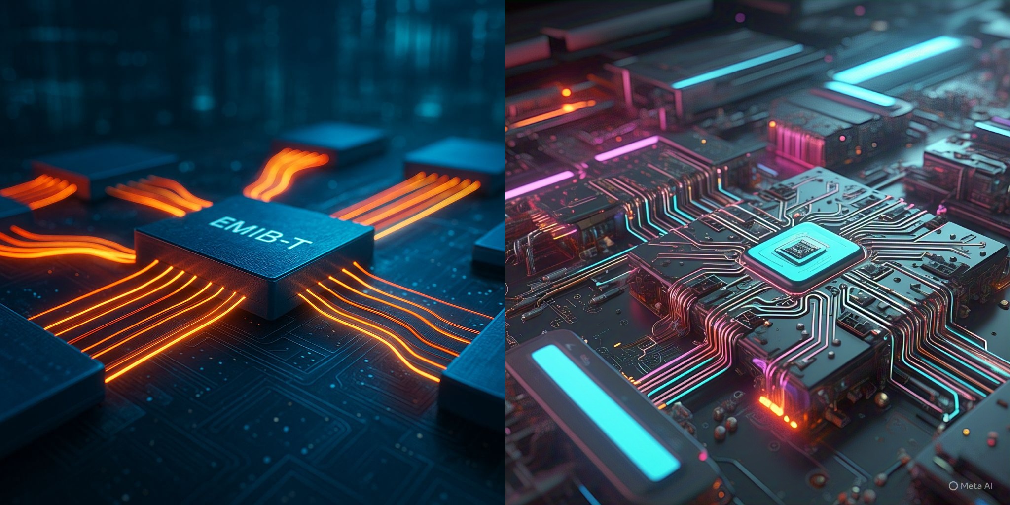
EMIB-T stands for Embedded Multi-die Interconnect Bridge-T—an advanced chip packaging tech developed by Intel. Think of it as a tiny silicon bridge that lets multiple chiplets talk to each other—fast.
Why is this a game-changer?
-
No giant interposers needed. That means lower costs and thinner packages.
-
Heterogeneous integration: Mix and match GPU, CPU, and AI accelerators in one package.
-
High bandwidth: Data flies between chiplets with minimal delay.
It’s like creating a custom superchip, one piece at a time.

🤝 Intel + Keysight: Teaming Up for the Future
So, what happens when Intel’s EMIB-T Technology meets Keysight’s EDA (Electronic Design Automation) tools?
Magic. Or rather, first-pass silicon success.
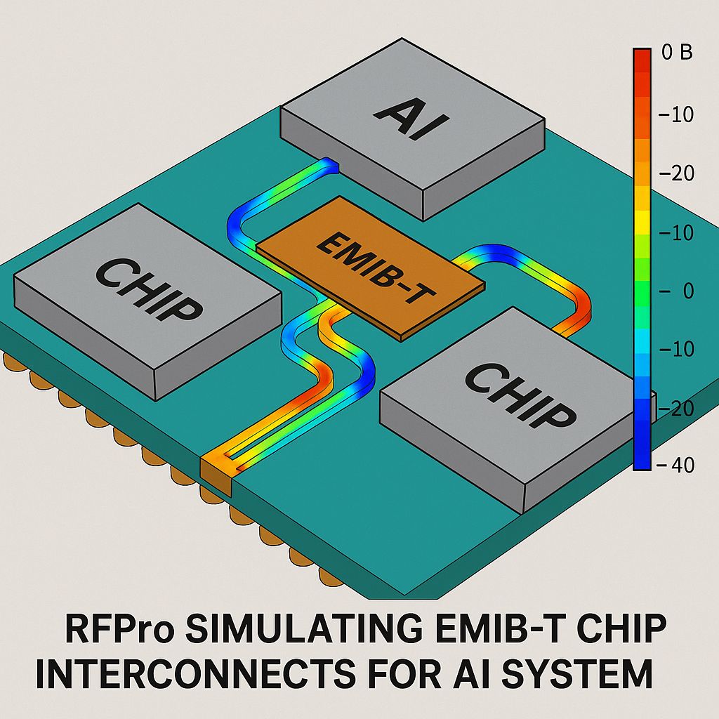
In April 2025, Intel Foundry and Keysight EDA announced their collaboration to integrate Keysight’s RFPro software with Intel’s 18A process. (Source – Keysight.com) ✅
Here’s what they’re unlocking:
-
Accurate electromagnetic simulations of chip-to-chip communication.
-
Thermal and mechanical stress validation for better reliability.
-
Improved design cycle time for AI and HPC applications.
You get all the performance with less trial and error—because in chip design, “guessing” is expensive.
🧠 Why EMIB-T Matters for AI and Data Center Growth
AI workloads are massive. GPUs are power-hungry. And server farms are hotter than a summer in Chennai.
So how does EMIB-T Technology help?
1. 🚀 Performance Boost
-
Superfast chiplet-to-chiplet communication
-
Reduced parasitics and interference
-
Lower latency = faster AI inferencing
2. 🧩 Modular Customization
-
Choose your own chiplet mix (CPU + GPU + AI core)
-
Ideal for data centers needing tailored AI architectures
3. 💰 Cost & Power Efficiency
-
Smaller footprint than interposers
-
Lower thermal output and energy consumption

Keysight’s EDA Tools: The Secret Sauce🧰
Why did Intel choose Keysight?
Keysight RFPro can simulate electromagnetic fields, thermal properties, and mechanical strain, all in a single EDA suite.
Here’s what’s included:
-
High-speed signal analysis for inter-chip connections
-
Layout-aware simulations for realistic design verification
-
Co-simulation with IC and packaging tools like ADS and PathWave
It’s like having an X-ray machine for your chip package—before you even manufacture it.
🧪 Real-World Impact: Who Benefits?
🖥️ AI Startups
They can prototype powerful custom silicon without a $500M fab.
🏢 Cloud Providers
Think AWS, Azure, GCP—scaling AI workloads with modular compute blocks.
🧬 HPC & Research Labs
Need extreme computing? EMIB-T scales it without needing massive monolithic chips.
Pros and Cons of EMIB-T Technology📊
| ✅ Pros | ❌ Cons |
|---|---|
| Modular chiplet integration | Still relatively new; limited adoption |
| High-speed, low-latency interconnects | Complex design flow without proper EDA tools |
| Lower cost than large interposers | Requires precise EM simulation for signal accuracy |
| Ideal for AI, HPC, and data centers | Dependent on Intel’s ecosystem and foundry roadmap |
EMIB-T Technology: 30+ FAQs (Frequently Asked Questions)📚
General FAQs
-
What does EMIB-T stand for?
EMIB-T stands for Embedded Multi-die Interconnect Bridge – Thermally Enhanced. It’s Intel’s silicon bridge packaging technology that enables efficient chiplet integration. -
How is EMIB-T different from standard EMIB?
EMIB-T is a thermally optimized version of EMIB, with enhancements for higher power density, better heat dissipation, and larger chiplet support. -
Why is EMIB-T important for AI and data centers?
It allows scalable, modular AI processors by connecting different chiplets—like CPU, GPU, and memory—with high bandwidth and low latency. -
Is EMIB-T a chip or a packaging technology?
It’s a packaging technology, not a chip. It acts as an ultra-thin bridge that links chiplets together on a single substrate. -
Which companies are using EMIB-T?
Intel is the primary developer. Keysight Technologies has partnered with Intel to enhance EMIB-T designs using EDA tools.
Technical FAQs
-
How does EMIB-T work?
EMIB-T uses a tiny silicon bridge embedded in the substrate to connect dies directly, bypassing traditional interposers or 3D stacking. -
What’s the benefit of not using an interposer?
Interposers are bulky, expensive, and generate more heat. EMIB-T avoids this, reducing cost, size, and power consumption. -
Can EMIB-T replace 3D stacking like Foveros?
Not exactly. EMIB-T is 2.5D. Intel often combines EMIB and Foveros in advanced designs for more flexibility. -
Is EMIB-T compatible with chiplets from different vendors?
Theoretically, yes, if they follow standard interfaces. Intel Foundry is promoting open standards for broader adoption. -
What design challenges come with EMIB-T?
-
Electromagnetic interference (EMI)
-
Thermal hotspot management
-
Precise alignment of chiplets
-
Signal integrity at high bandwidth
Simulation & Tools FAQs
-
How does Keysight support EMIB-T design?
Keysight provides RFPro, a tool that simulates the electromagnetic, thermal, and mechanical behavior of the silicon bridges. -
What is RFPro?
It’s a high-performance EM simulation tool integrated into Keysight’s ADS platform, used for packaging and interconnect analysis. -
Is EMIB-T easy to simulate with standard EDA tools?
No. Standard tools fall short. Multi-physics simulation is required—combining EM, thermal, and mechanical analysis. -
Does Intel offer a reference design for EMIB-T?
Intel Foundry Services (IFS) offers packaging reference flows, but full EMIB-T packages require custom optimization. -
Can startups access EMIB-T tools?
Through Intel Foundry partnerships and cloud-based EDA solutions, startups can get access, but it’s still resource-intensive.
Performance FAQs
-
What kind of bandwidth does EMIB-T support?
EMIB-T offers very high interconnect bandwidth, often exceeding 1 TB/s between chiplets. -
Does EMIB-T reduce latency?
Yes. It minimizes trace lengths between chiplets, reducing propagation delay and jitter. -
How does EMIB-T affect power efficiency?
Shortening chiplet communication paths and reducing power loss in long wires helps lower energy per bit transferred. -
Is EMIB-T thermally stable under load?
EMIB-T includes thermal optimizations, but requires good heat spreaders, vias, and airflow in final designs. -
Can EMIB-T support high-density AI compute arrays?
Yes. It’s ideal for AI accelerators, NPUs, and multi-die GPU clusters in hyperscale environments.
Integration & Manufacturing FAQs
-
How is the EMIB-T bridge manufactured?
It’s fabricated as a separate die and embedded in the substrate during advanced packaging. -
Does EMIB-T increase yield in chip production?
Yes. By splitting functionality across chiplets, you can reject bad dies without wasting entire monolithic chips. -
Can EMIB-T work with older nodes like 7nm?
Absolutely. EMIB-T is node-agnostic—it’s about package-level integration, not transistor size. -
How does EMIB-T affect thermal design power (TDP)?
It reduces system TDP by improving heat spread, but the final TDP still depends on chiplet density and workload. -
Is EMIB-T scalable for future compute demands?
Yes. It allows stacking more chiplets horizontally, and even vertically when combined with 3D technologies.
Market & Ecosystem FAQs
-
Is EMIB-T an open standard?
Intel is moving toward open chiplet interfaces (e.g., UCIe), but full EMIB-T packaging is still proprietary. -
What industries benefit most from EMIB-T?
-
AI and Machine Learning
-
Cloud and Edge Data Centers
-
High-Performance Computing (HPC)
-
5G/6G Telecom
-
Is EMIB-T used in consumer electronics?
Not yet widely. It’s more prevalent in high-end servers, AI accelerators, and research labs. -
What’s the cost of implementing EMIB-T?
Less than interposer-based solutions, but still high due to simulation, packaging, and testing complexities. -
What’s next for EMIB-T?
Integration with Foveros, chiplet marketplaces, and foundry-scale packaging ecosystems from Intel and partners like Keysight. -
Can EMIB-T support memory-on-package like HBM?
Yes. Many designs use EMIB-T + HBM to enable ultra-fast memory access for AI workloads.
Final Thoughts: Is EMIB-T the Future of Computing?🧾
Yes. And no.
If you’re building custom silicon for AI, HPC, or cloud workloads, EMIB-T Technology offers a massive leap in packaging innovation. But it’s not plug-and-play. You need advanced tools (like Keysight’s EDA suite) and a deep understanding of EM behavior.
The Intel–Keysight partnership shows that innovation doesn’t just happen in silicon—it’s the tools, teamwork, and timing that make the magic real.
External DoFollow link: ✅ Keysight Press Release